DFM & Technical Consulting
Pre-production circuit design audits to lower manufacturing risks, optimize assembly yield, and reduce unit costs.
01. Optimization Capabilities
Design for Manufacturing (DFM): Comprehensive pre-fabrication checks including layer-stackup balance analysis, copper weight distribution, annular ring validation, and trace-to-copper clearance reviews.
Design for Assembly (DFA): Component spacing audits to eliminate pick-and-place collision risks, footprint pad optimization, and shadow-zone mitigation during reflow soldering.
Supply Chain Lifecycle Analysis: Scrubbing the project Bill of Materials against live international databases to flag End-of-Life (EOL), obsolete, or long-lead-time components early.
Thermal & EMI Risk Mitigation: Board-level layout modeling to trace high-speed return paths, identify thermal hotspots, and implement defensive shielding before laboratory testing.
02. Core Focus Areas
Yield Optimization: Adjusting panelization layouts and breakaway rail configurations to maximize raw material utilization at the factory level.
Footprint Verification: Precise 1:1 cross-checking of all custom CAD land-patterns directly against active manufacturer physical component datasheets.
03. Project Deliverables Package
DFM Audit Report: A structured checklist identifying specific layout risks paired with detailed, actionable physical correction plans.
Corrected CAD Files: Original schematics and board layout databases updated with all approved safety and manufacturability improvements.
Alternative Sourcing Matrix: A curated list of drop-in, footprint-compatible alternative parts for volatile or high-risk active semiconductors.
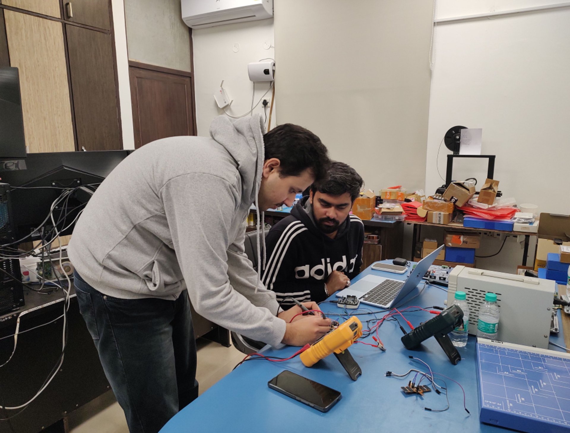
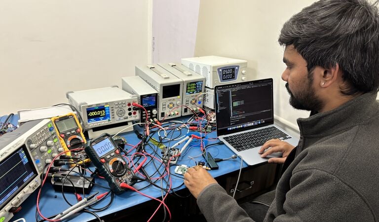
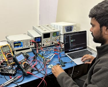
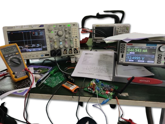
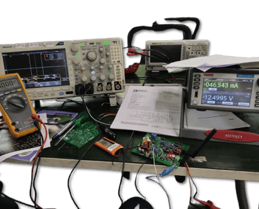
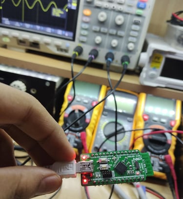
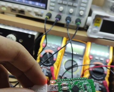
Recent Project Snapshots
A brief reference of our engineering optimization capabilities, demonstrating structural layout corrections, multi-rail thermal management audits, and pre-production hardware de-risking.
Project 01
Project 02
Project 03
Contact
Reach us for precise PCB design help.
© 2025. All rights reserved.
2181 Sector 28, Faridabad,
Haryana 121008.
Contact : +91 9899977637, 7982725030
Email : contact@ubyte.in, contact.ubyte@gmail.com
Our other active website