High-Speed PCB Design & Hardware Architecture

Engineering multi-layer, high-density physical platforms for automotive, industrial, and mixed-signal embedded systems.

01. Structural Capabilities

  • High-Density Multi-Layer Routing: Advanced placement and routing for complex, space-constrained 4 to 12+ layer architectures featuring fine-pitch microcontrollers, dense bus escapes, and optimized layer stackups.

  • Automotive & Industrial VCU Design: Proven expertise in engineering rugged Vehicle Control Units (VCUs) built to handle harsh electrical environments, high-current paths, switching relays, and dense power distribution networks.

  • Signal & Power Integrity (SI/PI): Strict control over trace impedance, differential pair routing, cross-talk mitigation, and strategic ground plane isolation to prevent signal corruption.

  • Mixed-Signal & RF Isolation: Rigid geometric partitioning between high-power switching tracks, sensitive digital compute cores, and on-board wireless systems (Wi-Fi/BLE) with custom antenna matching networks.

02. Integrated Subsystem Expertise

  • Industrial Communication Buses: Specialized low-noise routing and terminating networks for reliable field communication protocols including CAN (Controller Area Network) and LIN interfaces.

  • Compute & Memory Architectures: High-speed routing for external Flash memory blocks, dedicated EEPROM chips, and hardware debugging ports (JTAG and SEGGER J-Link interfaces).

  • Power Rails & Driver Subsystems: Structural layout of integrated buck/boost step-down power regulation circuits (12V down to 5V/3.3V) and thick-copper power delivery paths.

03. Engineering Toolstack & Standards

  • ECAD Environments: Altium Designer, KiCad Pro, Autodesk Eagle

  • Simulation Engines: HyperLynx (Signal Integrity), LTspice Circuit Simulation

  • Design Compliance: Rigid adherence to IPC Class 2 and Class 3 manufacturing standards, alongside pre-compliance rules for EMI/EMC.

04. Manufacturing Deliverables Package

Every completed project delivers a production-ready, factory-validated database:

  1. Fabrication Data: Gerber X2, ODB++, and IPC-2581 production files.

  2. Assembly Data: Validated Bill of Materials (BOM) featuring verified Manufacturer Part Numbers (MPN) and XY pick-and-place coordinates.

  3. Mechanical Data: High-precision 3D STEP files of the fully populated PCBA for physical enclosure matching.

High-Speed PCB Design & Hardware Architecture

A brief reference of our execution capabilities, demonstrating complex multi-layer routing, signal isolation, and industrial-grade hardware architecture.

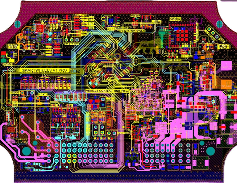
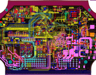
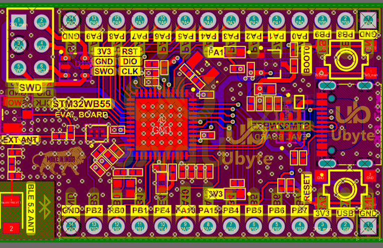
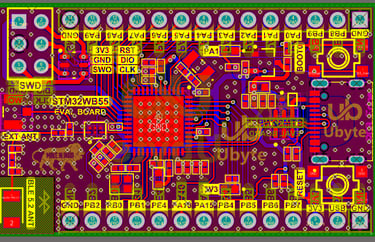
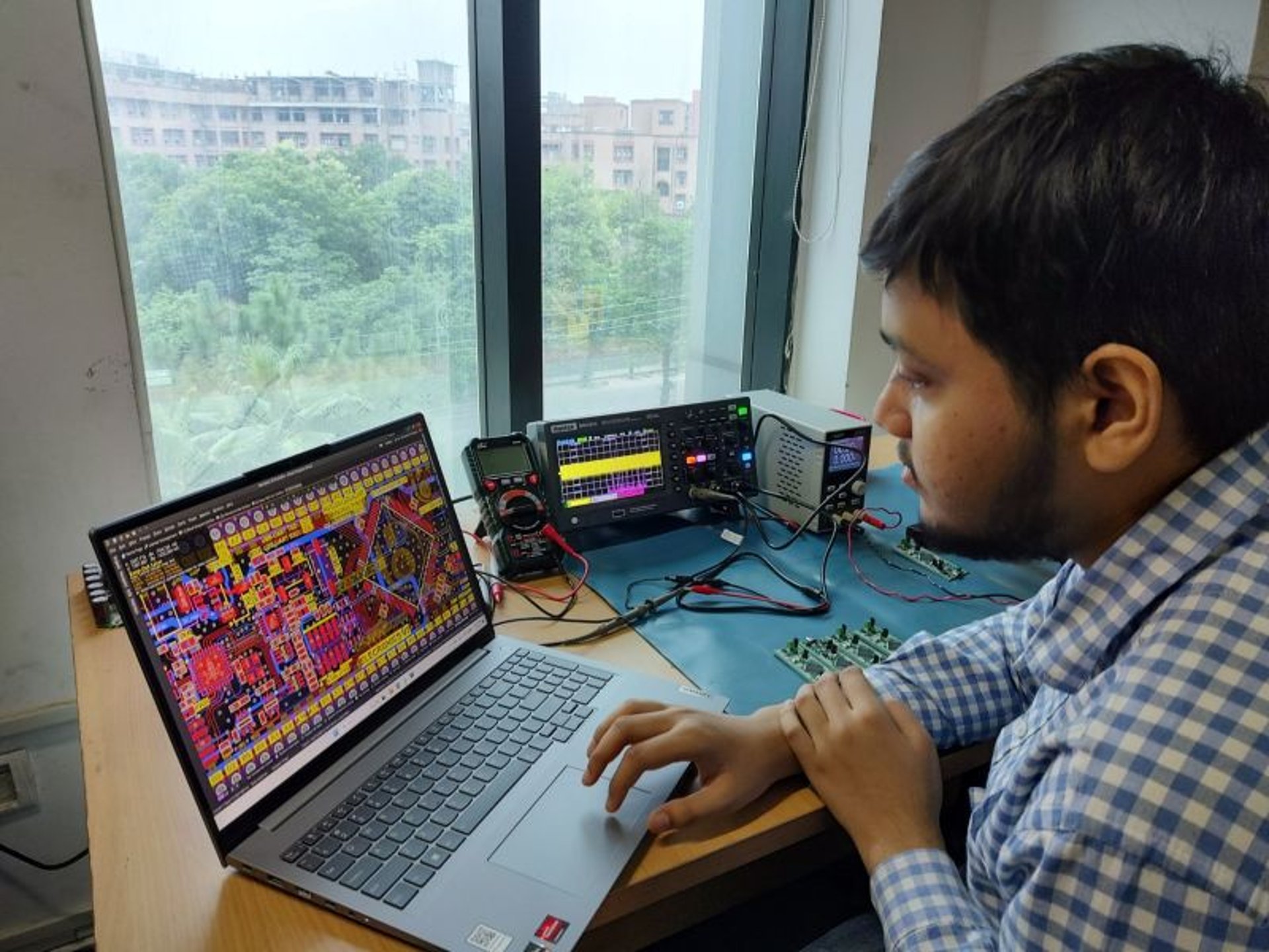
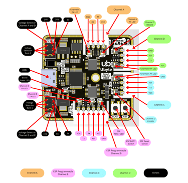
UBYTE Quad Channel USB to UART Converter
  • Classification: High-Density Interface Bridge

  • Architecture: Compact multi-channel layout optimized for clean, isolated high-baud-rate serial communication.

  • Key Engineering Milestones:

    • Parallel Bus Isolation: Precision routing of four independent UART channels, eliminating cross-talk and data corruption between simultaneous high-speed serial streams.

    • Multi-Rail Voltage Matrix: Clean power distribution layout supporting selectable 1.8V, 3.3V, and 5V logic level domains across a compact footprint.

    • Power Handling: High-integrity USB Type-C power input delivery path layout with local decoupling, transient suppression, and thermal dissipation routing.

    • Development Infrastructure: Geometric integration of dense ESP32 manual boot override structures and reset switch arrays without disrupting primary signal paths.

Project: SmartWheel V1.1 Pro
  • Classification: Automotive Vehicle Control Unit (VCU)

  • Architecture: Multi-layer high-density interconnect layout engineered for high-vibration and electrically noisy environments.

  • Key Engineering Milestones:

    • Fieldbus Integration: Low-noise routing and impedance-terminated networks for reliable CAN and LIN master/slave communication lines.

    • Mixed-Signal Partitioning: Rigid geometric isolation separating the sensitive compute core, on-board Wi-Fi/BLE wireless antenna networks, and high-current relay switching paths.

    • Power Architecture: Distributed layout for buck-boost step-down power regulation circuits handling stable 12V down-conversion to 5V and 3.3V power rails.

    • Hardware Diagnostics: Integrated on-board trace architecture for real-time debugging utilizing JTAG and SEGGER J-Link interfaces.

Recent Project Snapshots

STM32WB55 Eval Board

  • Classification: Ultra-Compact Wireless Development Platform

  • Architecture: Breadboard-compatible, high-frequency RF layout optimized for low-power wireless communication.

  • Key Engineering Milestones:

    • RF Front-End Engineering: Precision coplanar waveguide routing and impedance-matched network design for an on-board BLE, Zigbee, and Thread chip antenna.

    • Form-Factor Minimization: Dense, dual-layer trace layout engineered into a streamlined, high-density grid suitable for direct breadboard deployment.

    • Mixed-Signal Routing: Isolated placement and trace routing of digital user controls (switches) and high-frequency PWM switching logic for RGB LED modules.

    • Multi-Protocol Coexistence: Optimized grounding structure and layer referencing to maintain signal integrity across parallel 2.4GHz wireless communication stacks.

Contact

Reach us for precise PCB design help.

© 2025. All rights reserved.

2181 Sector 28, Faridabad,
Haryana 121008.
Contact : +91 9899977637, 7982725030
Email : contact@ubyte.in, contact.ubyte@gmail.com

Our other active website

Navigation